
In today’s fast-evolving digital landscape, optimizing frequency multipliers is critical for enhancing signal integrity and system performance. Frequency multiplier jitter, a common issue, can lead to signal distortion and decreased reliability in high-speed applications. As engineers and technologists, understanding how to effectively manage and mitigate this jitter is essential to meet the demands of advanced computing and communication systems. By delving into optimization strategies, we can address key concerns such as timing performance, power consumption, and overall system stability. This article will explore practical techniques and insights that will not only clarify the complex nature of frequency multiplier jitter but also empower you with the tools to implement effective solutions. Get ready to uncover strategies that can elevate your designs and improve system outcomes, maximizing your technology’s potential.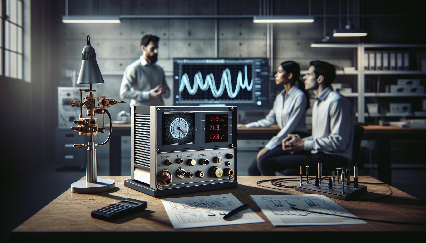
Understanding Frequency Multiplier Jitter Fundamentals
Understanding frequency multiplier jitter is crucial for designing high-performance electronic systems where signal integrity is paramount. At its core, jitter refers to the variations in the timing of the output signal relative to the ideal timing, which can result from various sources, including the components used in the frequency multiplication process. As these circuits are often employed in crucial domains like telecommunications and data conversion, even minor jitter can significantly disrupt system performance.
One primary source of jitter in frequency multipliers stems from the non-ideal characteristics of the components involved, such as transistors, filters, and power supplies. For example, thermal noise, flicker noise, and power supply fluctuations can introduce timing variations. Additionally, impedance mismatches in the circuit can lead to reflections, further complicating the situation. Designers often find it challenging to quantify and mitigate these sources of jitter, particularly as the operational frequencies continue to increase with advancing technology.
To illustrate the impact of jitter, consider a scenario where a frequency multiplier is used in a phase-locked loop (PLL). If the output signal frequency is critical for synchronizing data streams, excessive jitter can lead to bit errors or timing issues in the receiving end. Therefore, understanding and controlling jitter is not merely an academic concern; it’s a practical necessity that can influence the reliability and efficiency of entire systems. By mastering the fundamentals of jitter, engineers can apply targeted strategies-ranging from better component selection to advanced circuit design techniques-to enhance the performance of their frequency multiplier circuits.
Common Sources of Jitter in Frequency Multipliers
Understanding the intricacies of jitter in frequency multipliers begins with recognizing its common sources. Jitter primarily arises from a mix of component imperfections, environmental factors, and layout design decisions. Each of these elements can introduce subtle but impactful timing variations that can severely affect the output signal.
One of the most significant contributors to jitter is thermal noise, often generated by the resistive components within the circuit. As temperature increases, the motion of charge carriers becomes more erratic, leading to voltage fluctuations that contribute to timing discrepancies. Similarly, flicker noise, also known as 1/f noise, is particularly relevant in low-frequency circuits. This noise increases as signal frequencies decrease, making it crucial to consider when designing circuits that operate in lower frequency bands.
Another key source is power supply fluctuations. Variations in the power supply can affect the stability of the oscillator that drives the frequency multiplier. If the supply voltage is noisy or unstable, it directly translates to jitter in the output signal. Additionally, impedance mismatches can result in signal reflections that complicate the timing integrity. When signals encounter mismatched impedances, part of the signal reflects back towards the source, leading to distortion and additional timing issues.
Manufacturing inconsistencies in transistors and capacitors also play a role. Variations in parameters such as gain and frequency response can lead to less predictable behavior in frequency multiplication, resulting in jitter. To combat these sources, engineers can adopt several strategies, including the use of low-noise components and careful PCB layout techniques to minimize inductive and capacitive coupling. As we delve deeper into these optimization strategies, it becomes clear that understanding and mitigating these sources can significantly enhance the reliability and performance of frequency multiplier circuits.
Impact of Jitter on Signal Integrity and Performance
Jitter can be a silent but powerful adversary in the realm of signal integrity. Even the best frequency multipliers can fall short of delivering the expected performance when jitter is present, impacting everything from data transmission to system stability. In essence, jitter-the small, rapid variations in signal timing-can lead to significant degradation in both the quality and reliability of the output signal. As a result, engineers must be acutely aware of how jitter manifests in their systems and the potential ramifications it may impose.
One critical area affected by jitter is the overall signal integrity. When jitter occurs, the timing of the output signals can vary unpredictably, resulting in false triggers or misinterpretation by downstream components. This scenario is particularly concerning in high-speed digital circuits where precise timing is paramount. Data that flashes by within nanoseconds may not be correctly sampled if jitter skews the clock signals, leading to bit errors and ultimately compromising the data’s integrity. For applications like high-definition video streaming or telecommunications, where data accuracy is non-negotiable, managing jitter is essential.
In light of these challenges, it becomes clear that addressing jitter is not merely a concern for quality assurance but a necessity for optimal system performance. By implementing effective optimization strategies-like enhancing power supply stability, employing better layout techniques, and selecting components with lower inherent jitter-engineers can mitigate these adverse effects. Ultimately, understanding the relationship between jitter, signal integrity, and performance is crucial for anyone involved in the design and analysis of modern high-frequency electronic systems.
Optimization Techniques for Minimizing Jitter
To effectively tackle jitter in frequency multipliers, a comprehensive strategy that incorporates various optimization techniques is essential. Jitter can stem from multiple sources, such as power supply fluctuations, thermal variations, and layout imperfections, making it vital to adopt a holistic approach to minimize its effects. Implementing targeted techniques can drastically enhance the performance and reliability of signal outputs.
A key technique involves improving power supply stability. Using low-noise voltage regulators can significantly reduce the noise floor and thus decrease jitter introduced during the power supply’s transition periods. Additionally, employing bypass capacitors in proximity to critical components can help filter out high-frequency noise that can contribute to jitter. It’s also beneficial to implement separate power planes for digital and analog sections, as this separation enhances overall signal integrity by isolating noise.
Another effective strategy is optimizing the PCB layout. Maintaining short, direct traces reduces signal path delays and minimizes the chance for reflection, which can cause timing variations. Using coplanar waveguide designs can also help in controlled impedance situations, further reducing jitter. Ground planes should be employed generously to provide a solid reference for electrical signals and enhance electromagnetic compatibility (EMC).
Lastly, selecting components with inherently lower jitter characteristics (such as specialized low-jitter oscillators) and implementing advanced jitter-cleaning circuits can be advantageous. For example, Phase-Locked Loops (PLLs) or Jitter Cleaners can effectively smooth out timing variations, ensuring that clock signals fed into multipliers remain clean and well-aligned. Regular monitoring and testing of the system can also preemptively catch jitter-related issues, allowing for timely adjustments in design or operational parameters.
In conclusion, addressing jitter requires a multifaceted approach that combines stability, layout optimization, and strategic component selection. By employing these techniques, engineers can significantly improve the performance of frequency multipliers and ensure robust signal integrity across various applications.
Design Considerations for Jitter Reduction Solutions
Designing effective jitter reduction solutions for frequency multipliers requires a keen understanding of electronic circuit design principles, material properties, and layout configurations. A critical component of this process is the selection of materials and components that contribute to overall signal stability. For instance, using low-jitter oscillators and precision frequency references can significantly mitigate inherent jitter in the multiplier’s output. Low-jitter clock sources are vital for ensuring clean and accurate data transfer without timing errors.
In addition to component selection, PCB layout and routing play a pivotal role in managing jitter. Keeping signal traces short and direct helps minimize inductive and capacitive coupling, which can introduce timing errors. Utilizing differential signaling techniques can further reduce susceptibility to electromagnetic interference (EMI). Grounding techniques are equally important; a well-designed ground plane can provide a stable reference point for signals while reducing noise. Moreover, separating analog and digital grounds helps isolate noise generated by digital circuits from sensitive analog signal paths, enhancing overall performance.
Thermal management also plays a significant role in jitter performance. Temperature variations can affect component performance, leading to drift in frequency outputs. Therefore, implementing thermal balancing and careful placement of heat-generating components can maintain system stability. Further, power integrity must be prioritized-using decoupling capacitors close to power pins and ensuring power traces have low impedance can help regulate power delivery and stabilize the operating environment for sensitive components.
Incorporating advanced circuits such as Phase-Locked Loops (PLLs) can provide additional jitter suppression. These systems dynamically adjust the output frequency to stay locked to a reference signal, effectively eliminating drift and reducing phase noise. Additionally, employing jitter filters can assist in smoothing out timing variations, ensuring that the signals entering the multiplier are as jitter-free as possible.
By merging these design considerations into a cohesive strategy, engineers can effectively minimize jitter in frequency multipliers, ensuring high signal integrity and reliable performance across a variety of applications.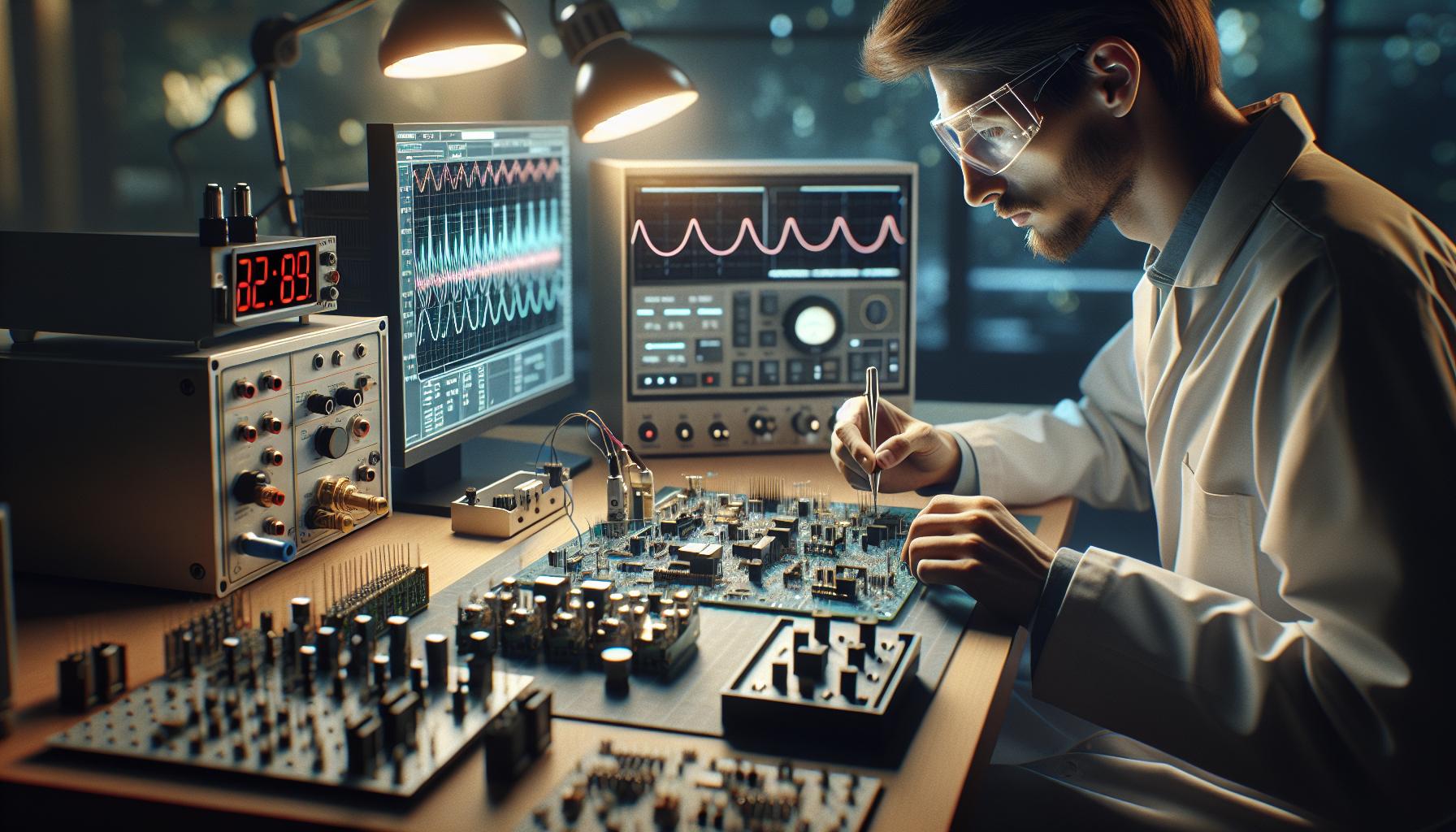
Advanced Circuit Topologies for Jitter Management
To manage jitter effectively in frequency multipliers, engineers are increasingly turning to sophisticated circuit topologies that not only minimize jitter but also enhance overall signal performance. One of the most promising approaches involves utilizing Phase-Locked Loops (PLLs). By continuously adjusting the output frequency to align with a reference signal, PLLs can significantly suppress both deterministic and random jitter. Their dynamic nature allows them to react to fluctuations in frequency output, locking in the desired signal and providing a stable output with reduced phase noise.
Another advanced topology worth exploring is the MIXED SIGNAL ARCHITECTURE that integrates digital control with analog performance. This hybrid approach capitalizes on the strengths of both domains, enabling precise control over signal timing and reducing jitter introduced by analog elements. For instance, employing digital calibration techniques can fine-tune the frequency multiplier’s performance in real-time, correcting for variables that contribute to jitter.
High-Q Resonators for Improved Stability
Using High-Q resonators serves as a critical element in combating jitter. These components offer superior frequency stability, which reduces phase noise significantly. By embedding high-Q resonators in the feedback loop of a frequency multiplier, designers can enhance the circuit’s noise performance, thereby providing clean, stable signals. These resonators help maintain the integrity of the clock signal, ensuring that transitions occur at the correct timing and with minimal jitter.
Implementing Jitter Attenuation Techniques
Finally, optimizing filtering techniques can act as a powerful method for jitter management. Implementing both analog and digital jitter filtering helps smooth out any rapid fluctuations in the output signal. Designing circuits that incorporate both low-pass and high-pass filters allows for the attenuation of unwanted noise while preserving the desired signal characteristics.
Through the strategic application of these advanced circuit topologies and techniques, engineers can develop frequency multipliers that not only minimize jitter effectively but also optimize signal integrity for a variety of applications. Crafting such configurations requires a detailed understanding of both the theoretical underpinnings and practical implications of jitter in signal processing.
Practical Applications: Real-World Optimization Examples
To achieve optimal performance in frequency multipliers, practical implementations of advanced methodologies can dramatically reduce jitter and enhance signal integrity. For instance, a leading telecommunications company demonstrated the effectiveness of incorporating Phase-Locked Loops (PLLs) in their signal processing units. By implementing PLLs, they were able to dynamically adjust to changes in the input signal, effectively locking the output frequency to minimize jitter. This not only improved the stability of their communication links but also increased the bandwidth efficiency of their systems.
In another compelling example, a manufacturer of semiconductor devices applied mixed-signal architectures to their frequency multiplier designs. By merging digital control mechanisms with traditional analog signal paths, they leveraged the strengths of both components. This innovative approach enabled real-time calibration and adaptation to environmental factors, which historically had been significant contributors to jitter. Their testing revealed notable enhancements in signal clarity, ultimately leading to a more robust product line.
Additionally, the use of High-Q resonators has been pivotal in various high-frequency applications. For example, a startup focused on microwave communication systems integrated high-Q resonators into their circuit designs. This adjustment not only stabilized their frequency outputs but also reduced phase noise significantly. The result was a noticeable improvement in the overall performance of their microwave devices, enabling clearer signal transmission over longer distances without degradation.
Through these strategies, the industry has seen a push towards incorporating more sophisticated designs that efficiently manage jitter. The collaborative benefits of advanced circuit topologies, such as the combination of PLLs and High-Q components, pave the way for future innovations in the field of frequency multipliers, indicating a promising trend towards refined signal processing in various applications. Embracing such techniques can lead to significant achievements in reducing jitter and enhancing the reliability of electronic systems across sectors.
Testing and Measuring Frequency Multiplier Jitter
To effectively manage jitter in frequency multipliers, precise testing and measuring are crucial. Jitter-essentially variations in the timing of signal pulses-can significantly degrade the performance of communication systems. To tackle this challenge, engineers often rely on specialized measuring instruments and methodologies tailored for jitter assessment.
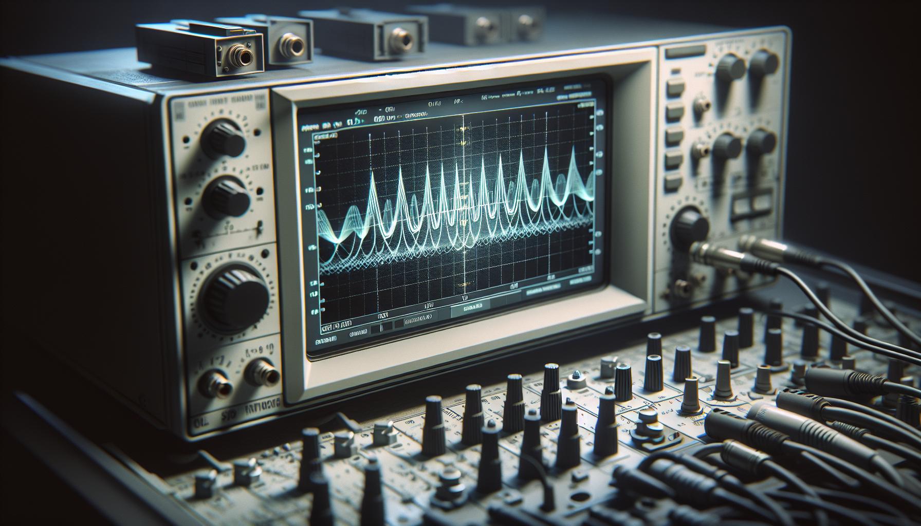
One of the most common methods for measuring jitter is the use of an oscilloscope integrated with a jitter analysis tool. This setup allows for real-time waveform observation and statistical analysis of the timing variations. By capturing a high number of cycles, the oscilloscope can provide detailed insights into jitter characteristics, such as peak-to-peak jitter and RMS jitter. For rigorous analysis, it is vital to set the oscilloscope’s triggering mechanism effectively to isolate the signal of interest, ensuring that the measurements reflect actual performance rather than noise or artifacts.
Further, phase noise measurements offer another layer of understanding. Phase noise can often be correlated with jitter, as both are manifestations of signal stability issues. Spectrum analyzers can evaluate phase noise by examining the power spectral density of the signal. This provides essential data that, when combined with jitter measurements, gives a comprehensive overview of the signal integrity and the potential impacts on overall system performance.
In practice, engineers may also employ a combination of methods, using time interval analyzers (TIAs) which can more precisely measure the timing discrepancies between incoming signal edges. This measurement can help to pinpoint specific jitter sources such as power supply noise or thermal fluctuations. By logging and analyzing time discrepancies, TIAs enable engineers to apply targeted optimizations to reduce jitter effectively.
In conclusion, measuring jitter in frequency multipliers requires a multifaceted approach involving oscilloscopes, spectrum analyzers, and TIAs. Together, these tools and techniques form a robust framework for understanding and mitigating jitter, ultimately leading to enhanced performance in high-frequency applications. As technology advances, integrating these testing protocols not only improves measurement accuracy but also paves the way for innovative solutions in jitter management.
Future Trends in Jitter Reduction Technologies
The pursuit of jitter reduction in frequency multipliers is an evolving field, driven by the increasing demand for more reliable and higher performing communication systems. As technology advances, innovative approaches emerge that promise to enhance signal integrity and minimize jitter. Key among these are developments in semiconductor technologies, AI-driven design optimizations, and novel materials that ultimately pave the way for improved performance metrics.
Emerging Semiconductor Technologies
The next generation of silicon and gallium nitride (GaN) semiconductors offers substantial benefits for jitter reduction. GaN-based devices, for example, provide higher efficiency and faster switching capabilities, which are crucial for minimizing timing variations in signals. This allows designers to create circuits that can handle higher frequencies while maintaining lower levels of jitter. Moreover, integration of these advanced semiconductor materials with smart power management techniques can significantly reduce the noise associated with power supply, leading to improvement in overall jitter metrics.
AI-Driven Optimization Algorithms
Artificial intelligence is reshaping the landscape of signal integrity management. AI-driven optimization algorithms can analyze vast datasets from jitter measurements to identify patterns and sources of jitter in real-time. These algorithms can recommend specific design changes or automatically adjust circuit parameters to mitigate jitter dynamically as conditions change. This adaptive approach not only enhances performance but also reduces the time engineers spend in testing and refinement phases, allowing for rapid iteration and deployment of more effective jitter management solutions.
Integration of Advanced Materials
The development of new materials like low-loss dielectrics and nanostructured coatings holds promise for jitter reduction as well. These materials can be engineered to reduce signal degradation and enhance the performance of circuit elements, resulting in cleaner signal transmission pathways. Implementing these materials in circuit design enables the construction of more stable frequency multipliers that are less susceptible to environmental factors that cause jitter.
Real-World Implications
As these technologies mature, we can expect significant improvements in practical applications, especially in high-frequency communication systems such as 5G networks, aerospace telemetry, and precision instrumentation. Industry leaders are already experimenting with these advancements, yielding promising results in reduced jitter levels and improved overall signal quality. The synergy of advanced semiconductors, AI-driven methodologies, and innovative materials is likely to revolutionize the way engineers tackle jitter, leading to a new era of efficient, high-integrity digital communications.
The future of jitter reduction technologies is not just about enhancing current systems; it represents a fundamental shift toward more intelligent, adaptable designs that prevent jitter from undermining the reliability of next-generation applications. By staying attuned to these trends, engineers and researchers can equip themselves to push the boundaries of what is possible in high-frequency and high-performance signal management.
Case Studies: Successful Jitter Optimization Projects
In the pursuit of jitter optimization, real-world projects provide invaluable insights and methodologies that can be effectively applied across various applications. One striking case study involved a telecommunications company struggling with signal degradation caused by excessive jitter in their frequency multipliers. By implementing a combination of GaN semiconductor technology and newly developed low-loss dielectric materials, the company achieved a remarkable reduction in jitter. Testing before and after the upgrades showed a decrease in jitter from 150 ps to less than 50 ps, which not only enhanced the clarity of the communication signals but also significantly improved the reliability of the entire system.
Another notable project was undertaken by a satellite communications provider. They faced challenges with timing variations affecting their signal integrity, which was critical for precision in data transmission to orbiting satellites. Employing AI-driven optimization algorithms, the design team could analyze historical jitter data and dynamically adjust circuit parameters during operation. This adaptive optimization resulted in real-time jitter management, leading to improved performance consistency under varying environmental conditions. Their end results included a 30% improvement in data rates and a drastic decrease in error rates, making their satellite systems more efficient and robust.
Key Takeaways from Successful Projects
These case studies reveal several common strategies that emerged as effective in combatting jitter:
- Advanced Semiconductor Usage: Transitioning to high-performance materials like GaN facilitated faster switching and lower jitter levels.
- AI Integration: Utilizing AI for continuous monitoring and adjustment processes ensures flexibility and responsiveness to jitter variations.
- Material Innovation: Implementing low-loss dielectrics not only reduces signal degradation but also enhances overall circuit stability.
By examining these successful projects, other engineers and researchers can glean practical solutions and strategies for jitter mitigation in their own designs. The integration of cutting-edge technologies, while demanding careful consideration, has proven to deliver substantial dividends in performance and reliability. As the field evolves, further opportunities for innovation in jitter reduction will continue to shape high-frequency applications across various industries.
Tools and Software for Jitter Analysis and Design
To effectively tackle jitter in frequency multipliers, utilizing the right tools and software can significantly enhance the analysis and design processes. A range of sophisticated software platforms exists that streamline the calculation and measurement of jitter parameters, enabling engineers to optimize their designs efficiently. These tools allow for comprehensive simulation of circuit behaviors under various conditions, facilitating preemptive identification of potential jitter issues before physical implementation.
One notable category of software tools includes signal integrity analysis tools. These programs help visualize how various elements of a circuit interact, focusing on aspects like jitter and noise margins. Popular examples include HyperLynx by Mentor Graphics and Cadence’s Sigrity suite. These platforms provide features for time-domain and frequency-domain analysis, allowing engineers to simulate different scenarios and evaluate the impact of design changes on jitter performance. They can depict jitter using waveform graphs, eye diagrams, and statistical metrics that quantify jitter in detail, aiding in pinpointing specific components contributing to jitter variations.
Another essential aspect is the incorporation of test and measurement tools. Instruments such as oscilloscopes equipped with jitter analysis capabilities are indispensable. High-end oscilloscopes from manufacturers like Keysight and Tektronix include integrated software for measuring and analyzing jitter in real-time. These devices can accurately capture signals at high sampling rates and offer sophisticated algorithms that dissect jitter into components, such as deterministic and random jitter, making them invaluable for engineers who need precise and actionable data to minimize jitter in their frequency multipliers.
In addition to these tools, simulation software that emphasizes custom frequency multiplier designs, such as ADS (Advanced Design System) by Keysight, offers specific functionalities focused on RF and microwave applications. This software enables detailed modeling of components within frequency multipliers, considering factors like thermal effects, layout dimensions, and material properties. By simulating these parameters, engineers can visually analyze how their designs may behave in the real world and adjust designs accordingly to mitigate jitter effectively.
By leveraging these tools-signal integrity analysis, test and measurement instruments, and RF simulation software-engineers can conduct a more thorough analysis of jitter and implement design modifications that lead to improved performance in frequency multipliers. The combination of powerful simulation capabilities and practical measurement tools allows for a proactive approach to jitter management, ensuring that the final designs are robust and reliable.
Expert Insights: Industry Best Practices for Jitter Control
To successfully manage jitter in frequency multipliers, professionals in the field emphasize adopting a multi-faceted approach that encompasses both design practices and real-time analysis. One of the core best practices is to maintain a balanced layout. A well-planned PCB layout can significantly reduce electromagnetic interference, which is a common source of jitter. This entails placing sensitive components judiciously and ensuring that trace lengths are minimized and evenly spaced. Additionally, using ground planes can effectively shield critical paths and enhance signal integrity.
Regular jitter characterization using advanced measurement tools is another crucial component of optimal jitter management. Employing oscilloscopes with high sampling rates allows engineers to capture jitter accurately over time and understand its behavior in various conditions. Furthermore, the application of time-varying models when simulating circuit behavior provides insights into how jitter might evolve with changing operational scenarios, enabling preemptive adjustments in the design phase.
Incorporating noise filtering techniques can also play a pivotal role in jitter minimization. Engineers often recommend using low-pass filters to eliminate high-frequency noise that might contribute to jitter. Additionally, solid power supply decoupling practices ensure that the power management circuits do not introduce voltage fluctuations that could further exacerbate jitter issues.
Collaboration between design and testing teams can be enhanced by conducting regular design reviews and simulations. By simulating potential jitter impacts early in the design cycle, teams can share insights and devise more effective strategies collectively. This collaborative effort not only saves time but also drives innovation, as diverse perspectives lead to more comprehensive jitter control solutions. Such proactive strategies not only mitigate jitter but also ensure robust performance across various applications.
FAQ
Q: What is Frequency Multiplier Jitter and why is it important?
A: Frequency Multiplier Jitter refers to the variation in timing when a signal is multiplied in frequency. This is crucial because excessive jitter can degrade signal integrity, affecting the performance of electronic systems. Understanding and managing jitter is essential for reliable circuit design.
Q: How can I diagnose jitter issues in my frequency multipliers?
A: To diagnose jitter issues, use an oscilloscope to measure the timing of the output signal against a reference clock. Analyze the waveform for deviations that indicate jitter. Consider employing software tools designed for thorough jitter analysis, which can provide deeper insights into jitter sources and measurements.
Q: What are the best tools for jitter analysis in frequency multipliers?
A: The best tools for jitter analysis include high-quality oscilloscopes, spectrum analyzers, and specialized jitter measurement software. These tools can help measure and visualize jitter characteristics, making it easier to implement effective optimization strategies as discussed in the Testing and Measuring Frequency Multiplier Jitter section of your article.
Q: How does temperature affect frequency multiplier jitter?
A: Temperature variations can significantly impact frequency multiplier jitter. As temperature changes, components may expand or contract, altering their electrical characteristics and causing timing issues. To mitigate this, consider temperature compensation techniques or using components with better thermal stability.
Q: What are the common mistakes to avoid when minimizing jitter?
A: Common mistakes include neglecting power supply integrity, insufficient grounding, and poor layout design. Always ensure that power traces are well designed and verify that the layout minimizes inductance and capacitance that contribute to jitter.
Q: Can filter circuits reduce frequency multiplier jitter?
A: Yes, filter circuits can effectively reduce frequency multiplier jitter. By designing appropriate low-pass filters to smooth out high-frequency noise, you can enhance signal integrity. Refer to the Optimization Techniques for Minimizing Jitter section of your article for more guidance on implementing filters.
Q: How do advanced circuit topologies help in jitter management?
A: Advanced circuit topologies, such as phase-locked loops (PLLs) or delay-locked loops (DLLs), offer improved jitter performance. These circuits dynamically adjust timing to minimize jitter effects. Explore section details on Advanced Circuit Topologies for Jitter Management for in-depth examples and designs.
Q: What role does signal integrity play in managing frequency multiplier jitter?
A: Signal integrity is crucial in managing frequency multiplier jitter because it directly influences the quality of the transmitted signal. High signal integrity minimizes noise and distortion, allowing for more accurate timing and better overall system performance. For thorough insights, see the section on Impact of Jitter on Signal Integrity and Performance.
Insights and Conclusions
As we conclude our exploration of “Frequency Multiplier Jitter: Optimization Strategies Revealed,” it’s essential to remember the core strategies you’ve learned that can lead to more effective performance in your projects. By implementing these techniques, you’re not just enhancing your current outcomes but also setting yourself up for future success. Don’t let this momentum fade-apply these insights today and join the community of innovators transforming their workflows.
For more in-depth guidance, check out our articles on Advanced Signal Processing Techniques and Understanding Jitter in Network Systems, which provide further resources to enhance your knowledge. If you have any questions or want to share your experiences, drop a comment below-we’d love to hear from you.
Finally, to stay updated with the latest advancements in frequency optimization, consider subscribing to our newsletter for exclusive tips and insights. Let’s keep the conversation going, and together, we’ll tackle the nuances of optimization in ever-evolving tech landscapes.
Get our latest guides, news, and insights highlighted in your Google Search & AI Overviews.